Diode Waveform Shaper wiring instructions, MOTM version
Posted 2/15/03 by John Loffink, updated
2/22/03
This page describes the Diode Waveform Shaper panel wiring.
I have decided not to use the headers but rather solder all
wires directly to the board. Over a long period of time, the headers
will just become a potential source of failure since the connections
are not gas tight. It appears easiest to solder the wires to the
PCB first, mount it to the bracket, then solder the wires to the
panel mounted components. This requires knowing the lengths of
the wires in advance, so these are listed below. You will want
to twist the sets of wires together, except when otherwise indicated,
for each component as they are soldered to the board, otherwise
you will have a huge rats nest of wires.
I had yellow, blue and gray wire in stock. Just substitute
whatever wire colors you have available. Use 22 gauge stranded
wire. Wire connections should be soldered to the PCB before the
PCB is mounted to the bracket. You then solder the connections
to the panel components.
Unfortunately, only one PCB connection is provided for each
of the positive and negative voltage references. Since chaining
the connections on the pots can be somewhat difficult, we will
instead use some unused summing op amp summing nodes on the PCB
as a "multiple" for the reference connections.
If you do have the PCB mount type pots, remember to add a piece
of shrink tubing over the wire before you solder it. Then you
can shrink this over the exposed connection, which also strengthens
it somewhat making the thin wires less prone to breakage.
On the twenty pin connectors P1-P4, the pin with square silk
screening around it is pin 1. The pin opposite it is pin 2. So
the one row is all odd numbered pins and the other row is all
even numbered pins. The wire lengths given below are long enough
to allow some slack in the wires so that they can be bundled and
tied down near the apex of the front panel and the PCB bracket.
-10V Reference
- P3-2 to R37 left pin (with power connector facing you) (blue,
2 inches)
+10V Reference
- P3-4 to R31 left pin (with power connector facing you) (yellow,
2.75 inches)
Limit switch, S1
- center tap to P4-2 (yellow, 7.5 inches)
- bottom tap to P4-1 (gray, 7.5 inches)
Gain pot, R18
- left terminal to P2-19 (blue, 9.0 inches)
- middle terminal to P2-18 (yellow, 9.0 inches)
- right terminal to P2-20 (gray, 9.0 inches)
Offset pot, R17
- left terminal to R34 left pin (-10V reference) (blue, 7.5
inches)
- middle terminal to P1-20 (yellow, 8.5 inches, do not bundle
with other wires)
- right terminal to R28 left pin (+10V reference) (gray, 7.5
inches)
Bkpt+1 pot, R3
- left terminal to R77 left pin (-10V reference) (blue, 6.5
inches, do not bundle with other wires)
- middle terminal to P3-18 (yellow, 7.5 inches)
- right terminal to P3-17 (gray, 7.5 inches)
Bkpt+2 pot, R7
- left terminal to R35 left pin (-10V reference) (blue, 6.5
inches, do not bundle with other wires)
- middle terminal to P3-10 (yellow, 7.5 inches)
- right terminal to P3-9 (gray, 7.5 inches)
Bkpt-1 pot, R1
- left terminal to R76 left pin (+10V reference) (blue, 5.5
inches, do not bundle with other wires)
- middle terminal to P1-16 (yellow, 6.5 inches)
- right terminal to P1-15 (gray, 6.5 inches)
Bkpt-2 pot, R5
- left terminal to R29 left pin (+10V reference) (blue, 5.5
inches, do not bundle with other wires)
- middle terminal to P1-8 (yellow, 7.5 inches)
- right terminal to P1-7 (gray, 7.5 inches)
Gain+1 pot, R4
- left terminal to P3-16 (blue, 7.5 inches)
- middle terminal to P3-14 (yellow, 7.5 inches)
- right terminal to P3-15 (gray, 7.5 inches)
Gain+2 pot, R8
- left terminal to P3-8 (blue, 6.5 inches)
- middle terminal to P3-6 (yellow, 6.5 inches)
- right terminal to P3-7(gray, 6.5 inches)
Gain-1 pot, R2
- left terminal to P1-14 (blue, 6.5 inches)
- middle terminal to P1-12 (yellow, 6.5 inches)
- right terminal to P1-13 (gray, 6.5 inches)
Gain-2 pot, R6
- left terminal to P1-6 (blue, 6.5 inches)
- middle terminal to P1-4 (yellow, 6.5 inches)
- right terminal to P1-5 (gray, 6.5 inches)
In jack, J1
- left terminal (tip) to P1-2 (blue, 10.5 inches)
- top terminal (tip NC) no connection
- beveled terminal (ground) to P1-1 (gray, 10.5 inches)
Mod+1 jack, J3
- left terminal (tip) to P3-20 (blue, 7.5 inches)
- top terminal (tip NC) to beveled terminal (jumper wire)
- beveled terminal (ground) to P3-19 (gray, 7.5 inches
Mod+2 jack, J5
- left terminal (tip) to P3-12 (blue, 6.5 inches)
- top terminal (tip NC) to beveled terminal (jumper wire)
- beveled terminal (ground) to P3-11 (gray, 6.5 inches)
Mod-1 jack, J2
- left terminal (tip) to P1-18 (blue, 8.0 inches)
- top terminal (tip NC) to beveled terminal (jumper wire)
- beveled terminal (ground) to P1-17 (gray, 8.0 inches)
Mod-2 jack, J4
- left terminal (tip) to P1-10 (blue, 7.5 inches)
- top terminal (tip NC) to beveled terminal (jumper wire)
- beveled terminal (ground) to P1-9 (gray, 7.5 inches)
Out+1 jack
- left terminal (tip) to 1K resistor soldered into R9 hole
(blue, 10.5 inches)
- top terminal (tip NC) to right terminal (yellow, 1.25 inches)
- beveled terminal (ground) to P4-17 (gray, 6.0 inches, not
wrapped with other two wires)
- bottom terminal (ring) to 49.9K resistor R9 (yellow, 10.5
inches)
- right terminal (ring NC) to top terminal (yellow)
Out+2 jack
- left terminal (tip) to 1K resistor soldered into R11 hole
(blue, 9.5 inches)
- top terminal (tip NC) to right terminal (yellow, 1.25 inches)
- beveled terminal (ground) to P4-15 (gray, 6.0 inches, not
wrapped with other two wires)
- bottom terminal (ringw) to 49.9K resistor R11 (yellow, 9.5
inches)
- right terminal (ring NC) to top terminal (yellow)
Out-1 jack
- left terminal (tip) to 1K resistor soldered into R2 hole
(blue, 8.5 inches)
- top terminal (tip NC) to right terminal (yellow, 1.25 inches)
- beveled terminal (ground) to P4-13 (gray, 5.0 inches, not
wrapped with other two wires)
- bottom terminal (ring) to 49.9K resistor R2 (yellow, 8.5
inches)
- right terminal (ring NC) to top terminal (yellow)
Out-2 jack
- left terminal (tip) to 1K resistor soldered into R3 hole
(blue, 7.0 inches)
- top terminal (tip NC) to right terminal (yellow, 1.25 inches)
- beveled terminal (ground) to P4-19 (gray, 5.5 inches, not
wrapped with other two wires)
- bottom terminal (ring) to 49.9K resistor R3 (yellow, 7.0
inches)
- right terminal (ring NC) to top terminal (yellow)
Out jack J10a (top)
- left terminal (tip) to P4-4 (blue, 4.5 inches) plus wire
to J10b below
- top terminal (tip NC) no connection
- beveled terminal (ground) to P4-3 (gray, 4.5 inches) plus
wire to J10b below
Out jack J10b (bottom)
- left terminal (tip) to J10a left terminal (blue, 1.75 inches)
- top terminal (tip NC) no connection
- beveled terminal (ground) to J10a beveled terminal (gray,
1.75 inches)
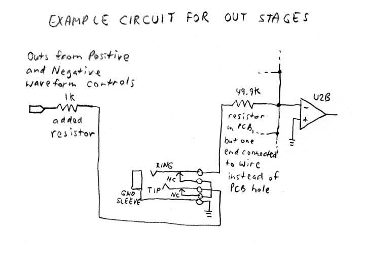
The individual OUT-+ stages are more complicated than your
standard connections. Referring to the shaper_ sch.pdf, the basic
idea is to take the outputs of the individual negative and positive
waveform controls and bring them to the output (tip) of the jack
through a 1K resistor. This connection is normalled to the right
tab on the jacks. This is a normally closed connection to the
ring connection, bottom tab. The ring connection then goes back
to the 49.9K summing resistors (R2, R3, R9, R11) feeding U2B.
This gives about a 2% gain error from the original design, but
since this whole thing is nonlinear anyway I figure it doesn't
matter. Here's a schematic of the basic
idea.
back